FREE DELIVERY on orders over £275 ex VAT
Micro-thermography Applications of the FOTRIC 616C R&D Test Station
With a thermal sensitivity of 0.05℃ and resolution up to 384, a 30°standard lens, and optional 50μm macro lens, the FOTRIC 616C R&D Test Station is mainly used for accurate thermal measurements on small components. Designed for engineering and product development, there are various micro-thermography applications of the FOTRIC 616C Test Station. It provides R&D solutions for printed circuit boards (PCB) and chip dissipation design. It can also detect defects in finished or semi-finished electronic products, and identify hot spots and heat anomalies in pharmaceutical, biomedical and material testing.
Examples of Micro-thermography Applications of the FOTRIC 616C R&D Test Station
PCB Monitoring
An infrared camera can quickly identify any components of a PCB that are consuming current, due to the heat generated when drawing current. Thermal inspection is an established procedure for failure detection and quality management. Used in both prototype development and serial production, the following detections can be identified:
- hotspots and atypical temperature distributions on the PCB surface and multichip modules due to incorrect mounting
- increased contact resistances caused by constriction of wires
- hidden cracks in joints
- power losses induced by RF mismatch
- incorrect thermal connections of heat sinks
- short circuits
- cold solder joints (insufficient tin during soldering).
The image below demonstrates how an imperfection in the circuit board (shown as a hotspot) was discovered. The heating process was monitored and recorded through FOTRIC AnalyzIR (Time: 0s, 6s, 9s, and 17s).

Chip Dissipation
Defective heat sinks can seriously affect chip performance and life. Overheating semiconductors may lead to a PN junction failure causing faults or failure in the device. Heat sinks work by transferring the heat created by a device ensuring the chip temperature stays within an appropriate range.
In the below example, an automotive headlight LED is being monitored. To continue operating properly, the LED chip temperature should not exceed 120°C due to the heat sink cooling the chip. If the heat sink is poorly designed or made of improper material, the heat dissipation will be seriously affected, thus shortening the chip service life or resulting in a change of LED colour.
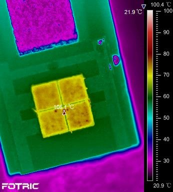
In the automotive headlight LED test, the red dots in the centre of the chip may gradually enlarge due to defective heat sinks, reducing the chip life. The AnalyzIR software is configured so an alarm will be triggered when the critical temperature of 120°C is exceeded.
Monitoring Small components in Electrical Products
A non-contact microscopic camera allows thermal analysis of extremely small structures in the micro-meter range. This provides a detailed representation of temperature distribution on complex electronic assemblies and components.
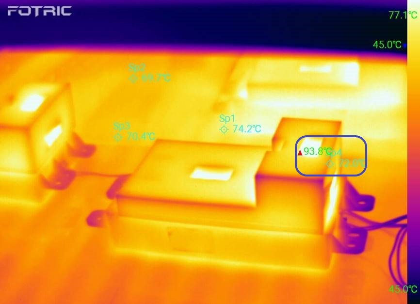
This image shows the TV module aging test carried out after the manufacturing process. The temperature reached 93.8 ℃ unexpectedly which would have resulted in rapid and premature aging and causing further product malfunctions.
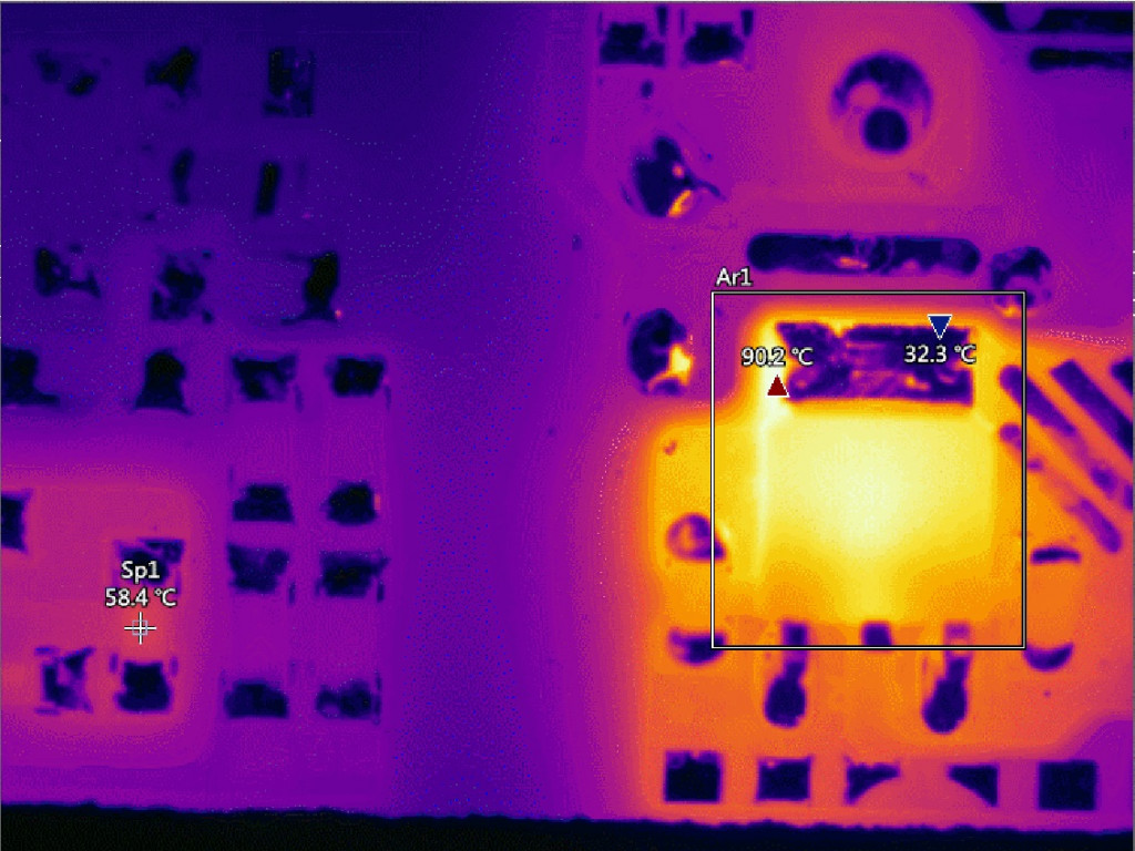
A faulty DC-to-DC converter is determined since the temperature reached 98.2 ℃ abnormally.
Other applications of using a thermal camera for such testing includes inspecting a circuit board with a cold solder joint, a defective semiconductor wafer, heat sink, LED, VCSEL, winding displacement, TV module, universal prototype board, atomizer heating wire of e-cigarette, DC converter of new energy vehicles, in-car microphone, etc.
Biomedical and Pharmaceutical Testing
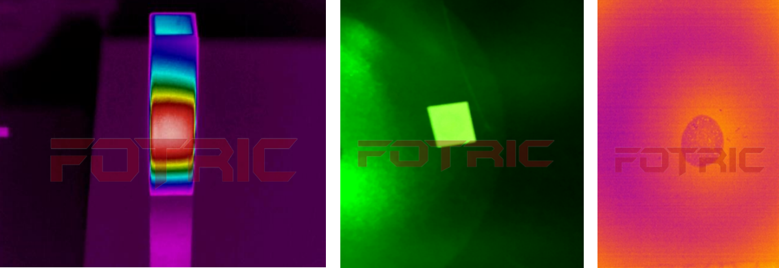
In this example of research on targeted nanomaterials, the 616C thermal camera with a 50μm macro lens is used. It tests and compares the solar thermal conversion efficiency of different targeted nanomaterials without interference before testing in vivo.
Materials Testing
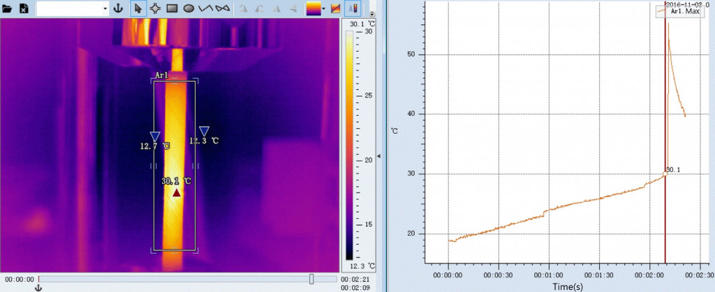
Lastly, in this example the 616C thermal camera can test the performance through temperature change of fibrous carbon material subjected to tension.
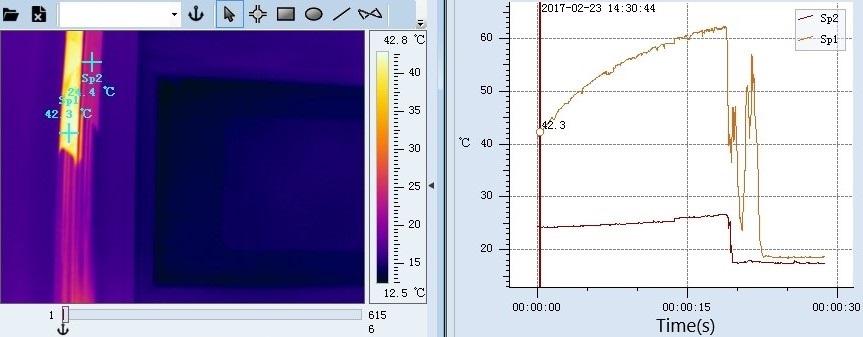
And test the thermal conductivity of two materials (two bars)as well.
For more information on the FOTRIC 616C R&D Test Station, please see the Product Page or contact us.
